
Minimizing PCB Artwork Defects Through DFM
One of the most frustrating moments in electronics development is when a seemingly flawless schematic leads to countless defects once it hits the SMT mass production line. There was not a single error in circuit theory, and everything looked perfectly aligned on the CAD screen—so where did it go wrong?
The answer is simple.
A schematic may indicate “perfect electrical connectivity,” but that does not guarantee “perfect manufacturability.” Located at the intersection of design and manufacturing, PCB artwork is far more than just connecting lines—it is the critical first step of DFM (Design for Manufacturability) that transforms a circuit from the virtual space of a monitor into a physical product.
How Subtle Differences in PCB Layout Make a Massive Impact⏲️
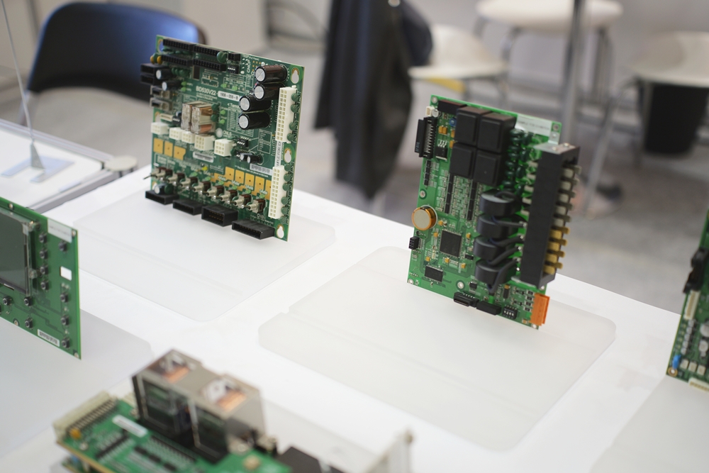
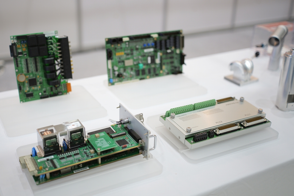
At a one-stop EMS facility, we witness firsthand the various manufacturing defects that occur every day when DFM is omitted during the PCB layout stage. There are three representative phenomena, starting with tombstoning. If the pad sizes on either side of a chip component differ, or if the thermal dissipation area of the copper pattern is unbalanced, a difference in surface tension occurs when the solder melts during reflow soldering. As a result, one side of the component lifts up, causing an open-circuit defect.
Next is solder bridging. When fine-pitch IC components or chips are placed too closely together, or when solder resist mask clearance is insufficient, molten solder flows into adjacent pins, causing a short circuit. These types of issues can never be caught during the schematic verification stage—they can only be prevented through DFM-oriented layout design.
3 Key Elements of DFM-Based PCB Layout✍🏻
To maintain a mass production yield of over 99%, the following key elements must be secured during the layout stage
🟣 Optimizing Footprints and Pad Balance
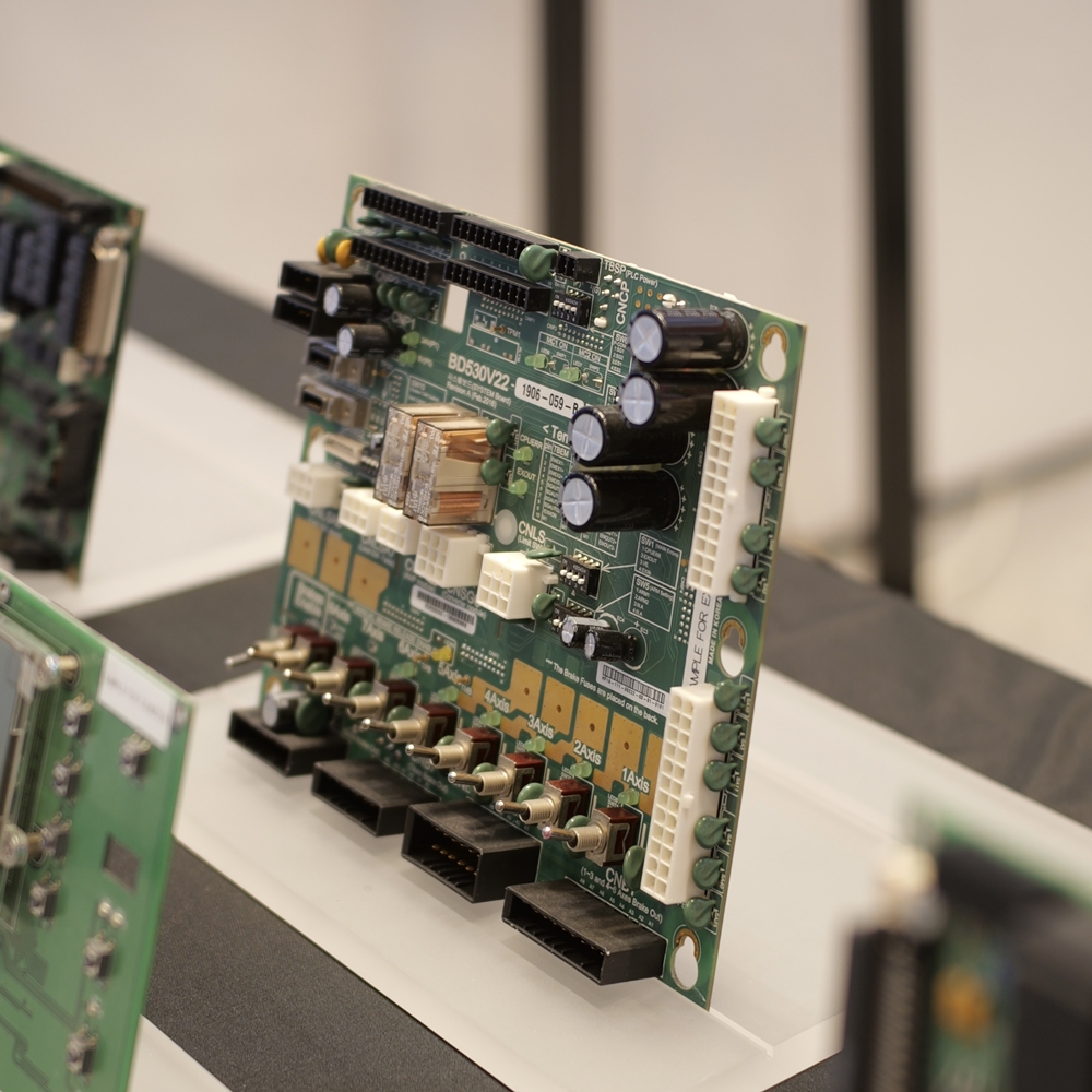
Pad dimensions and spacing must be finely adjusted to align with the precision of the SMT equipment, the characteristics of the solder paste, and the reflow temperature profile. For symmetrical chip components in particular, the thermal capacity of both copper patterns must be balanced so that the solder melts evenly at the same time.
🟣 Securing Component Placement and Clearance
Design must account for SMT nozzle paths, mechanical clearance based on component height, and accessibility for tools during manual assembly or touch-up. If capacitors or resistors are placed too close to connectors or taller components, neighboring parts can be damaged during future rework, or insufficient heat transfer during soldering can compromise overall assembly quality.
🟣 Strategic Placement of Test Points
PCB layouts that overlook ICT (In-Circuit Testing) or AOI (Automated Optical Inspection) lead to skyrocketing inspection costs. Placing test points at regular intervals on key signal and power lines allows probe pins to make stable contact, enabling fast and reliable 100% inspection after final assembly.
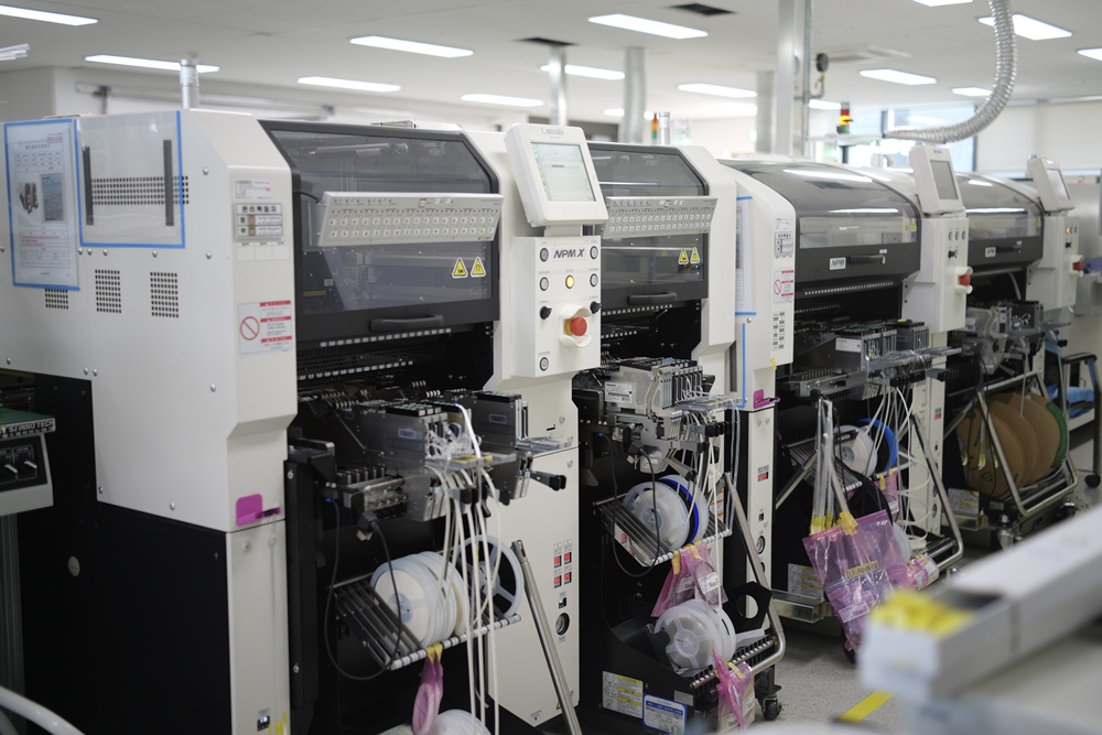
In a one-stop EMS model—where everything from PCB artwork design to SMT and final box-build assembly happens under one roof—layout designers never work in isolation. They receive real-time feedback in the very same space from SMT line engineers and quality control personnel. This structure, where shop-floor know-how is directly translated onto the CAD screen in real time, is the ultimate weapon for truly realizing Design for Manufacturability (DFM).
Good Layout Proves Its Worth on the Mass Production Line.
Its true value is proven when SMT mounter nozzles place components without stopping, when boards exiting the reflow oven pass AOI inspection on the very first try without a single fault flag, and when they fit perfectly into final product enclosures to operate reliably for years.
The fastest, most cost-effective way to ensure quality is not repairing defects after they happen, but validating every single trace line and component pad from a manufacturing perspective at the PCB layout stage using DFM.
Its true value is proven when SMT mounter nozzles place components without stopping, when boards exiting the reflow oven pass AOI inspection on the very first try without a single fault flag, and when they fit perfectly into final product enclosures to operate reliably for years.
The fastest, most cost-effective way to ensure quality is not repairing defects after they happen, but validating every single trace line and component pad from a manufacturing perspective at the PCB layout stage using DFM.